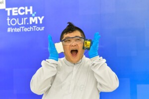
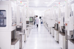
Earlier last week, Intel held its annual Tech Tour event and gave several media members a tour of its factories in Penang and Kulim. Suffice to say, it’s a privilege that many of us here have wished for, present company included, so when the opportunity arised, we naturally jumped at it. So, here’s a quick look at some of the rooms that we thought would be interesting to you.
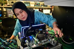
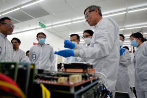
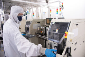
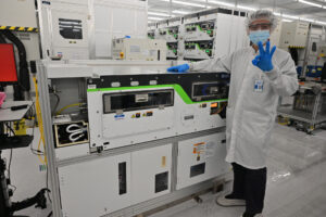
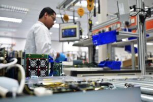
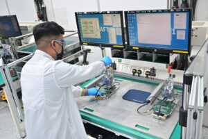
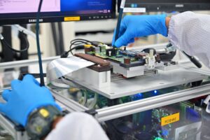
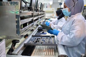
So, once stripped of our personal effects – we weren’t allowed to bring in our own electronics – and dressed up in bunny suits, the first room we were ushered into was the space designated simply by Intel as the Design and Development Lab.
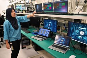
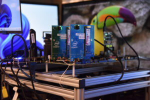
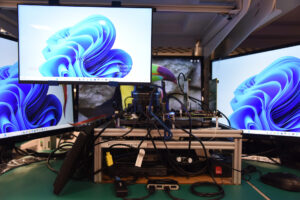
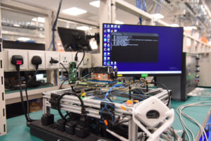
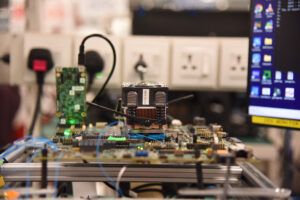
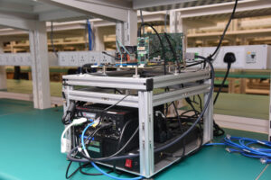
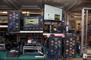
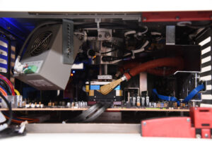
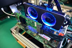
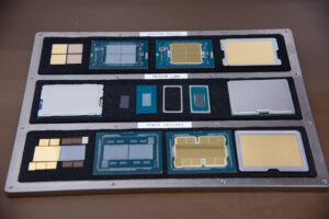
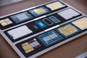
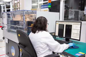
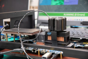
As a quick note, this area was the space that had by far the most amount of consumer-ready hardware. These included market-available power supplies from known brands, as well as some desktop casing from brands that I haven’t actually heard from in a while. That said, Intel explained that this room was where its engineers conducted a lot of testing with corresponding hardware to its processors, including laptop platforms. Some examples of the tests include performance and power consumption.
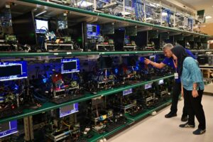
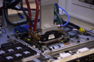
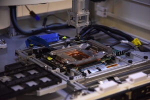
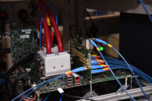
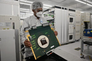
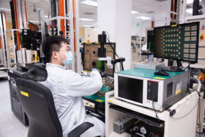
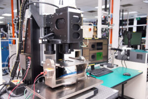
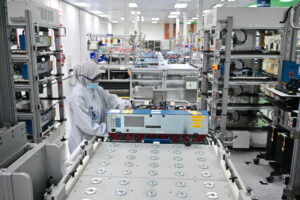
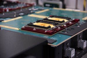
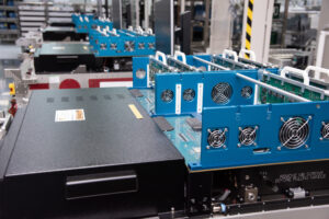
Another area that we visited as part of the Intel Tech Tour was the Penang Assembly and Test facility, otherwise known as PGAT. This section of the Intel facility is basically where the silicon dies from its die sort facilities end up to be assembled.
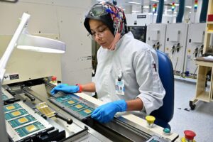
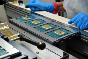
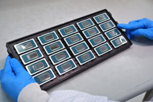
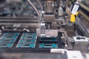
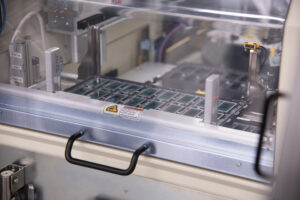
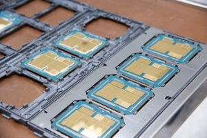
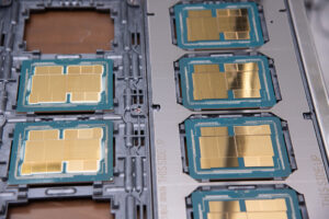
To put it simply, the PGAT is where Intel chips are formed, with dies being attached to PCB substrates with epoxy, a Ther Interface Material (TIM) is attached, and then followed by burn in, tests, and then run through a series of test conditions, across a multitude o platforms and operating systems.
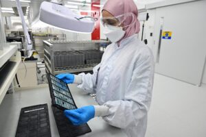
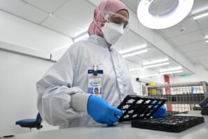
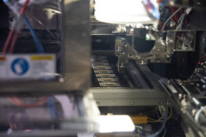
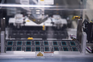
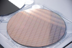
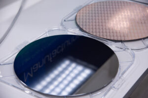
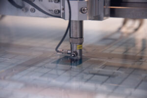
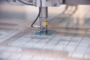
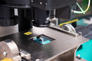
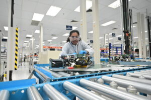
Speaking of die sorting, we were also taken to the Kulim Die Sort Die Prep (KMDSDP) facility across the state border in Kedah. This is where the all the dies in our silicon, just like Raptor Lake and soon, Meteor Lake. This is where a full 300mm circular wafer is taken and cut into individual chips, involving grinding laser scribing, and a factoryload of machines are put to task.
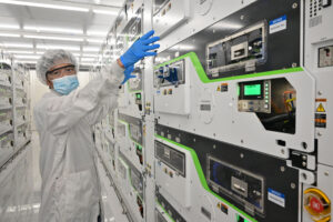
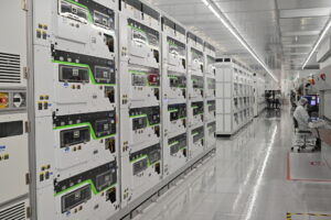
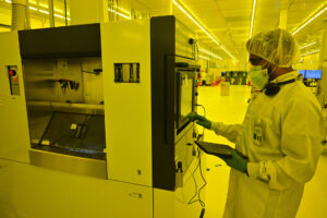
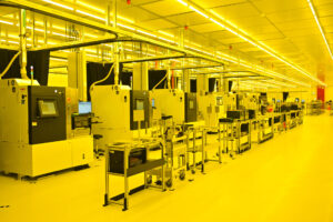
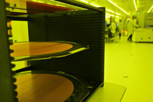
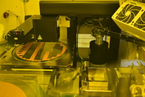
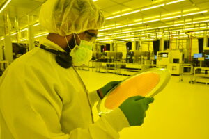
Fun fact, part of this facility is perpetually bathed in a special yellow light, and that is because the mylar tape used to hold the wafer in place is extremely sensitive to UV light, so much so that the engineers were to expose it to the outside sun or light, it would lose its structural integrity almost immediately. Think of the room being in a perpetual state of blue light filtration, but instead of your phone, it’s area wide. Another fun fact is that each chip is further tested on a probe card, using thousands of needles thinner than human hair.
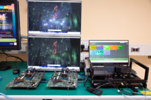
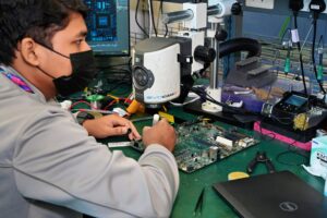
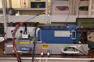
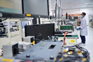
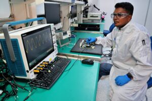
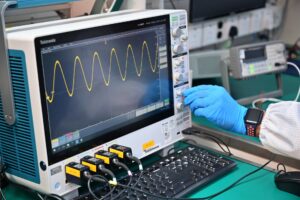
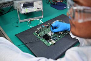
Of course, there’s also an on-site Failure Analysis lab at the Intel facility. This facility was pretty much self-explanatory, and we got to see how the broad strokes of how its engineers tested for product failure.
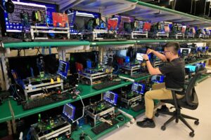
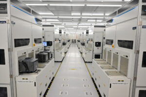
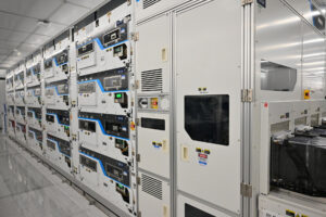
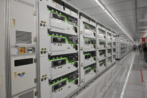
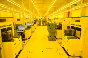
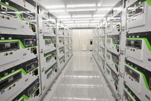
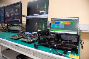
The last stop on our Intel factory tour was System Integration and Manufacturing Services (SIMS) division. Touted as a one-of-a-kind factory, this department is responsible of producing test equipment and boards for Intel fabs, factories, and labs globally.
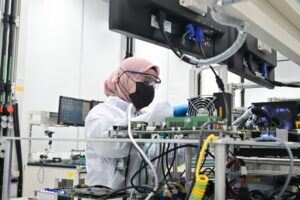
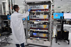
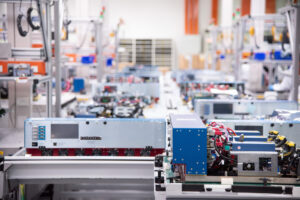
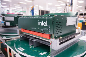
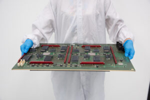
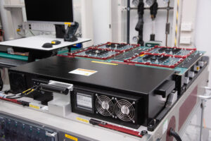
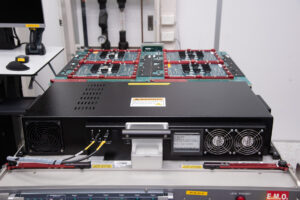
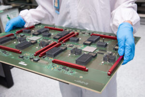
This facility is essentially equipped with tools and machines that allow it to perform Burn-In stress testing, allowing it feed exceedingly high temperatures and voltage on Intel CPUs; High Density Modular testing on new products development and CPU production ramping, as well as system level testers to ensure that the final product will function as it should, the minute it reaches the hands of consumers.
The post Photo Essay: Intel Tech Tour Malaysia 2023 appeared first on Lowyat.NET.


0 Commentaires